PA sequencing to avoid blow outs

PA sequencing to avoid blow outs

There have been many reports of the PA blowing up. The PA transistor is a MOSFET that can blow up due to high input voltages that can lead to the input gates blowing up or drawing too much current and blowing up the source-drain channel.

What is going on? 

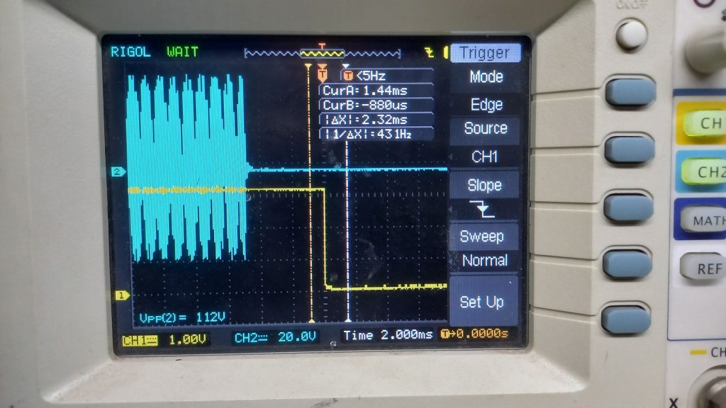
We applied an oscilloscope probe to the TX_LINE. The TX_LINE goes high under raspberry Pi control during transmission. We applied the second probe to a dummy load connected to the antenna socket. What we found is below.

sBITX PA spike on TX->RX

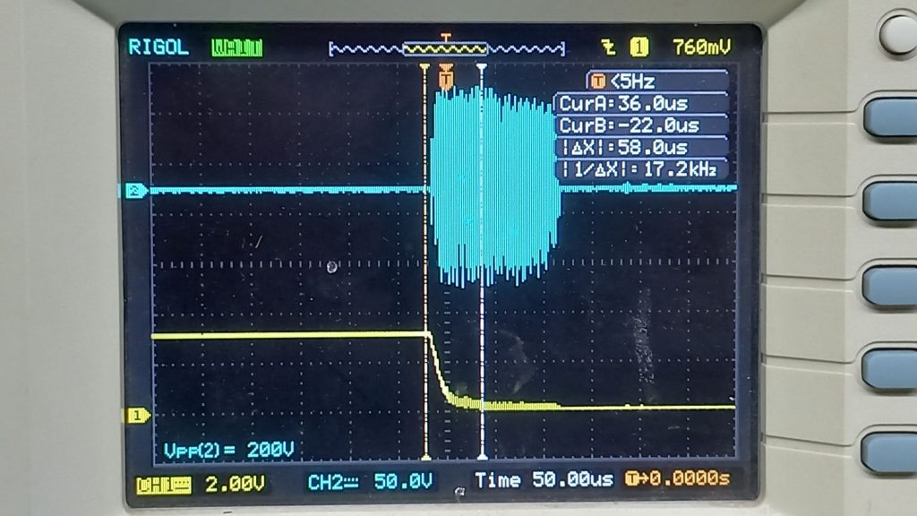
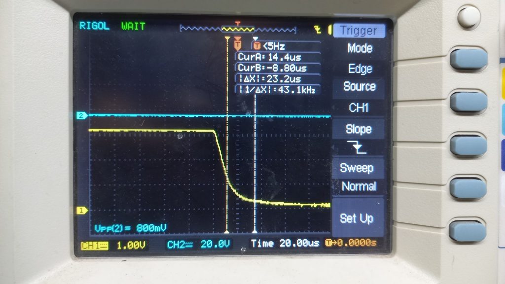
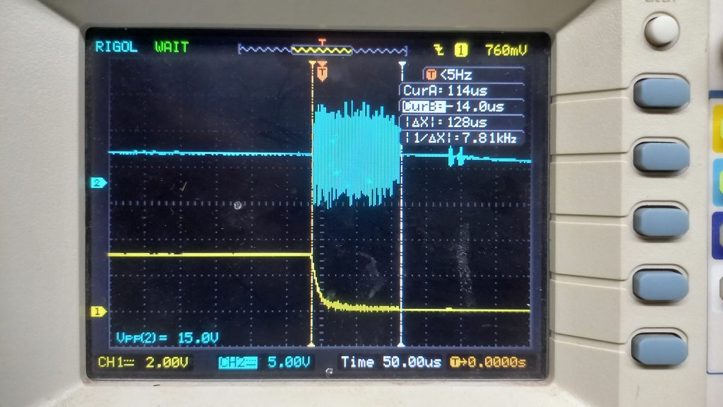
As you can see, there is an enormously high power spike of 220V peak to peak (more than 100 watts of power).  Even more telling is that the gate RF t has 20 volts of RF. The maximum rating for the gate is +/-20V as per the datasheet some of the spikes are hitting that as well. See below

PA Spike on the Gate

Why is this happening?

The power amplifier is permanently connected between the exciter portion and the harmonic filters. On receive, the power to the drivers and the bias is switched off and the relay K9 with U3 bypass the PA to directly the signal to the rest of the radio.

When the transmission ends, the TX_LINE goes low and the power to the PA is switched off, simultaneously, the relay K9 and the analog switch U3 are released, allowing the RF to flow back from the PA output to the input. The power amplifier takes a few hundred microseconds to power down as the bypass capacitors still hold charge. This sets up the oscillations that we are seeing. To confirm this, I desoldered C14 and the spike went away, (it also renders the receiver dead) by breaking the feedback loop.

The spike of the oscillations remains on for as long as the bypass capacitors of the PA hold charge and they quickly discharge, killing the oscillations. Not quickly enough  to do damage.

What is to be done?

The powering up and down of the PA has to be sequenced. When we switch to transmit, we must first switch off the relay and U3, give it a millisecond and then power up the PA. When transiting to receive from transmit, we have to follow the reverse sequence. First power down the PA, wait for the caps to discharge and then switch the relay K9 and the switch at U3 to bypass the PA.

How can it be done?

The PA power is turned on and off in the existing sBitx when TX_LINE goes high at the gate of Q10. Now, instead of the TX_LINE, we take another GPIO line (we can call it TX_POWER) to separately control the powering up and down of the PA. This makes the spike go away.

Four things to do: 

  1. We pull in the new code from github. This software mod does not impact the unmodded sbitx but it can potentially blow up the modified sBitx if this mod is not in place.
    Power on the sBitx, open the terminal with Ctrl-Alt-T and type the following:

    cd sbitx
    git pull
    ./build sbitx
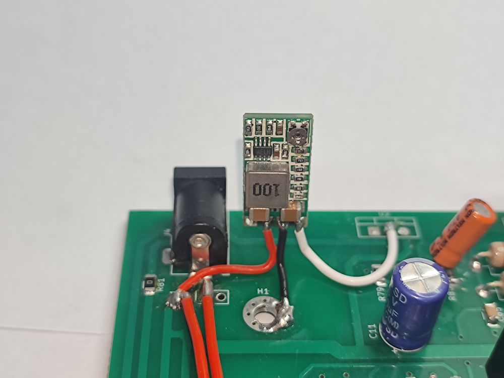
  2. We cut the track that brings the TX_LINE to the gate of the Q10 with a sharp knife.
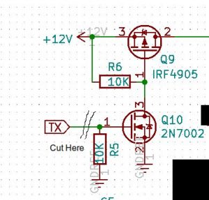
  3. We add a wire from the Gate of Q10 to be taken to pin 36 of the Raspberry Pi’s connector on the digital board.

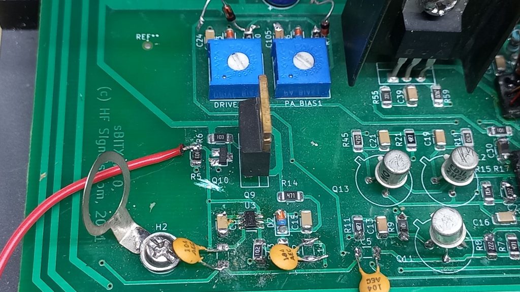
    Gate of Q10 isolated from TX_LINE and connected to TX_POWER
  4. We solder the wire coming from the Q10 gate to pin 36 of the Raspberry Pi’s connector on the digital board.

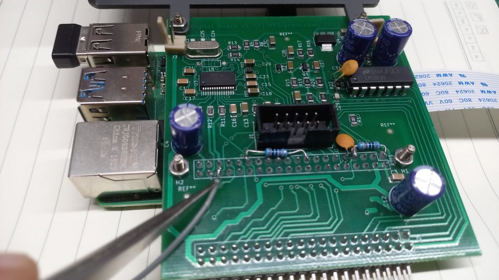
    Wire soldered to Pin 36 of RPI to connect to Q10 gate (TX_POWER)


Result

You can see that the spike is gone. The two pictures are taken with different timing bases to be sure.

PA showing no spike after the mod
PA output clean after the mod at greater resolution

sBitx Basic Kit Assembly Notes

sBitx Basic Kit Assembly Notes

Ken, N2VIP
Here are some photos/steps I took to assemble my sBitx “kit” (complete minus RPi 4 and Raspberry Official 7″ Display).
A reminder, here’s what’s included:
image9.jpeg
image11.jpeg
1) remove the front and top panel, being careful to not damage the wires attached to them. There is no reason to remove the back or bottom. Disconnect the speaker lead from the circuit board and put the top aside.
2) remove the back plate from the front panel, re-attach the back plate to the front panel. Connect the red lead included with the display to the 5v connection on the display board, the black lead to the GND connection. Do not attach the display ribbon cable (yet – it turns out it’s easier to attach the ribbon cable to the display later, trust me.)
image0.jpeg
3) Prepare the RPi 4 – insert the MicroSD card in the reader and attach the Display ribbon cable to the display connector on the RPi 4, the silver leads face “up” the blue tape is down, against the black ‘wedge’. If you are not familiar with these connectors, there is a wedge that lies against the circuit board – pull it out a tiny amount, don’t force it) the ribbon cable should just slide right in, then slide the ‘wedge’ into the connector.
image1.jpeg
4) Mount the RPi 4 to the digital board, being sure the 40 pins on the are correctly inserted into the socket (tip – if you can’t see any pins on top of the black connector, and you don’t feel any pins on the bottom of the black connector, you’ve got it right). The screw holes on the RPi 4 won’t match the standoffs on the digital board if the pins are not correct. (Again, the display ribbon cable should be installed before you secure the RPi 4)
image2.jpeg
5) Lean the front panel against the front of the chassis, twist (!) the display ribbon cable then insert it into the display connector, silver leads facing away from the circuit board, blue tape against display PCB.
image3.jpeg
Secure the front panel to the radio with the 4 screws you previously removed.
6) Connect the red lead from the display board to the lower power connector on the component side of the digital board, the black lead from the display board to the top pin as shown:
image4.jpeg
7) Re-attach the speaker connector to the three-pin connector on the digital board (it only attaches one way), then seat the top of the case back on top and secure it with the 4 screws you previously removed.
NOTE: HF Signals assembly instructions instruct you to use the included two pin jumper cable, soldering the wires to the pins on the display board, but the supplied jumpers that came with the display (red/black/yellow/green, female-female, about 7-8″ long) are just fine and should be secure for most users.
There were some leftover parts:
image5.jpeg
8) So then I applied 12v (13.8v) DC and my unit powered up!
image6.jpeg
Starting the sBitx application, you see this:
image8.jpeg
The wifi ‘burp’ is quite obvious, I know turning off wifi will stop that, but now to grab my mic from my uBitx and hook it up to an antenna.
Thanks to everyone at HF Signals, I’m very pleased with this build.
I hope these instructions help others decide if they want to buy a “kit” or “assembled” sBitx.

Upgrading to switching regulator (Development Edition)

Upgrading to switching regulator (Development Edition)

From Anthony Good, K3NG, Anil Rayporula, VU2DXA

The very early sBitx (Developer Edition) were shipped with a linear regulator, the LM338 to drop the voltage down from 13.8V power supply to the 5V needed by the Raspberry Pi and other digital circuitry.  This often led to heating issues. An upgrade kit was shipped to these users. These are the instructions to install it properly.

The new regulator looks like this:
 
1.  Take off the top panel and disconnect the speaker.  Lay this aside.
2.  Disconnect the white ribbon cable going from the Pi to the touch screen display.  There are little black tabs on each side of the connector on the display unit that need to pop straight out in the direction of the ribbon cable to release the ribbon cable.
3.  Disconnect the brown and black wire (touch display power) from the digital board.
4.  Remove the gray ribbon cable out of the digital board by pulling the gray ribbon straight backwards.
5.  Loosen the two nuts on the right side holding the metal bracket that the Pi and the digital board is mount to.  Do not take the nuts entirely off.
6.  Pull the Pi and digital board assembly straight up to remove and set aside.
7.  Remove the four screws holding the main board to the chassis
8.  Disconnect the two red wires from the power switch on the back panel
9.  Remove screws on the four back corners of the outside of the chassis to remove the back panel along with the main board.
10.  Put the rest of the chassis with the screen and controls aside.  Carefully place the back panel and main board on your workbench and loosen the three screws holding the bar that presses the two final transistors and the LM338 regulator on to the back panel heatsink.  Remove the bar and three screws.  The main board should be loose from the back panel now.
11.  Unsolder the LM338.  With the front of the main board facing you, it’s the first three pin device from the left on the back on the back that was against the heatsink.
12. Remove the main board screw at H1 and solder the black (ground) wire of the new switching regulator to the ground trace at H1, and replace the screw.
13. Solder the red switching regulator wire (+13.8 volt input) to the right-most pin where the LM338 used to be.  This is the input pin shown in the diagram below.
14. Solder the white switch regulator wire (output) to the middle pin, where the LM338 used to be.  This is the output pin shown below.  (The first pin of the LM338, labeled “Adjust” below, will remain open.
15.  Place the main board against the back panel.  Place the bar that presses the final transistors to the heatsink place.  Place the three screws back in, but do not tighten all the way.  Leave them rather loose.
16.  Place the main board and back panel together back into the main chassis.  Line up the three front jacks (mic, earphone, cw key) to the holes in the front panel.  Carefully push the back panel into place until it mates correctly with the side and bottom panels.
17.  Line up the main board with the four screw holes.  Place the four screws in, starting them, but leaving them slightly loose.  After all four are started, tighten all four.
18.  Tighten the three screws that are in the bar that presses the two final transistors on to the back panel heatsink.  Use your best judgement.  (I tightened until the two final transistors would not move with me pressing my finger nail on the side of them.)
19. (Optional step)  Connect the power.  Turn on the unit and use a voltmeter to verify that the white lead from the new switching regulator has about 5.4 volts on it.  If it is not close to 5.4 volts, stop and troubleshoot.  If it’s good, turn off the unit, disconnector the power, and proceed.
20.  Re-assemble the remaining parts of the unit.  Slide the pi and digital board subassembly back in, being sure to have the pins on the bottom meting correctly with the connector on the main board.  Be sure to connect the gray ribbon cable to the back of the digital board (it is keyed so it can be inserted only one way), the white ribbon cable to the display unit (blue side down, silver side out), and black & brown power cable for the display going to the digital board (brown is down, black is up).  The assembly manual has pictures that can help (https://www.hfsignals.com/index.php/sbitx-assembly-manual-v1-0/).
21.  Reinstall the top panel, connecting the speaker to the digital board prior to putting the top panel on.
22.  Connect the power, and power up!
This is how the installed regulator looks (installed on the PCB).  It has been photographed outside the box for better clarity.